
The Angstrom Era Begins: TSMC Shatters Records with $56 Billion Capex to Scale 2nm and A16 Production
In a move that has sent shockwaves through the global technology sector, Taiwan Semiconductor Manufacturing Company (NYSE: TSM) announced today during its Q4 2025 earnings call that it will raise its capital expenditure (capex) budget to a staggering $52 billion to $56 billion for 2026. This massive financial commitment marks a significant escalation from the $40.9 billion spent in 2025, signaling the company's aggressive pivot to dominate the next generation of artificial intelligence and high-performance computing silicon.
The announcement comes as the "AI Giga-cycle" reaches a fever pitch, with cloud providers and sovereign states demanding unprecedented levels of compute power. By allocating 70-80% of this record-breaking budget to its 2nm (N2) and A16 (1.6nm) roadmaps, TSMC is positioning itself as the sole gateway to the "angstrom era"—a transition in semiconductor manufacturing where features are measured in units smaller than a nanometer. This investment is not just a capacity expansion; it is a strategic moat designed to secure TSMC’s role as the primary forge for the world's most advanced AI accelerators and consumer electronics.
The Architecture of Tomorrow: From Nanosheets to Super Power Rails
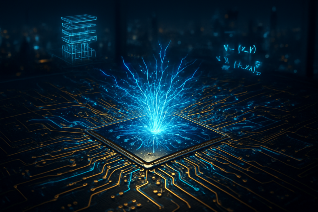
The technical cornerstone of TSMC’s $56 billion investment lies in its transition from the long-standing FinFET transistor architecture to Nanosheet Gate-All-Around (GAA) technology. The 2nm process, internally designated as N2, entered volume production in late 2025, but the 2026 budget focuses on the rapid ramp-up of N2P and N2X—high-performance variants optimized for AI data centers. Compared to the current 3nm (N3P) standard, the N2 node offers a 15% speed improvement at the same power levels or a 30% reduction in power consumption, providing the thermal headroom necessary for the next generation of energy-hungry AI chips.
Even more ambitious is the A16 process, representing the 1.6nm node. TSMC has confirmed that A16 will integrate its proprietary "Super Power Rail" (SPR) technology, which implements backside power delivery. By moving the power distribution network to the back of the silicon wafer, TSMC can drastically reduce voltage drop and interference, allowing for more efficient power routing to the billions of transistors on a single die. This architecture is expected to provide an additional 10% performance boost over N2P, making it the most sophisticated logic technology ever planned for mass production.
Industry experts have reacted with a mix of awe and caution. While the technical specifications of A16 and N2 are unmatched, the sheer scale of the investment highlights the increasing difficulty of "Moores Law" scaling. The research community notes that TSMC is successfully navigating the transition to GAA transistors, an area where competitors like Samsung (KRX: 005930) and Intel (NASDAQ: INTC) have historically faced yield challenges. By doubling down on these advanced nodes, TSMC is betting that its "Golden Yield" reputation will allow it to capture nearly the entire market for sub-2nm chips.
A High-Stakes Land Grab: Apple, NVIDIA, and the Fight for Capacity
This record-breaking capex budget is essentially a response to a "land grab" for semiconductor capacity by the world's tech titans. Apple (NASDAQ: AAPL) has already secured its position as the lead customer for the N2 node, which is expected to power the A20 chip in the upcoming iPhone 18 and the M5-series processors for Mac. Apple’s early adoption provides TSMC with a stable, high-volume baseline, allowing the foundry to refine its 2nm yields before opening the floodgates for other high-performance clients.
For NVIDIA (NASDAQ: NVDA), the 2026 expansion is a critical lifeline. Reports indicate that NVIDIA has secured exclusive early access to the A16 process for its next-generation "Feynman" GPU architecture, rumored for a 2027 release. As NVIDIA moves beyond its current Blackwell and Rubin architectures, the move to 1.6nm is seen as essential for maintaining its lead in AI training and inference. Simultaneously, AMD (NASDAQ: AMD) is aggressively pursuing N2P capacity for its EPYC "Zen 6" server CPUs and Instinct MI400 accelerators, as it attempts to close the performance gap with NVIDIA in the data center.
The strategic advantage for these companies cannot be overstated. By locking in TSMC's 2026 capacity, these giants are effectively pricing out smaller competitors and startups. The massive capex also includes a significant portion—roughly 10-20%—allocated to advanced packaging technologies like CoWoS (Chip-on-Wafer-on-Substrate) and SoIC (System on Integrated Chips). This specialized packaging is currently the primary bottleneck for AI chip production, and TSMC’s expansion of these facilities will directly determine how many H200 or MI300-class chips can be shipped to global markets in the coming years.
The Global AI Landscape and the "Giga Cycle"
TSMC’s $56 billion budget is a bellwether for the broader AI landscape, confirming that the industry is in the midst of an unprecedented "Giga Cycle" of infrastructure spending. This isn't just about faster smartphones; it’s about a fundamental shift in global compute requirements. The massive investment suggests that TSMC sees the AI boom as a long-term structural change rather than a short-term bubble. The move contrasts sharply with previous industry cycles, which were often characterized by cyclical oversupply; currently, the demand for AI silicon appears to be outstripping even the most aggressive projections.
However, this dominance comes with its own set of concerns. TSMC’s decision to implement a 3-5% price hike on sub-5nm wafers in 2026 demonstrates its immense pricing power. As the cost of leading-edge design and manufacturing continues to skyrocket, there is a growing risk that only the largest "Trillion Dollar" companies will be able to afford the transition to the angstrom era. This could lead to a consolidation of AI power, where the most capable models are restricted to those who can pay for the most expensive silicon.
Furthermore, the geopolitical dimension of this expansion remains a focal point. A portion of the 2026 budget is earmarked for TSMC’s "Gigafab" expansion in Arizona, where the company is already operating its first 4nm plant. By early 2026, TSMC is expected to begin construction on a fourth Arizona facility and its first US-based advanced packaging plant. This geographic diversification is intended to mitigate risks associated with regional tensions in the Taiwan Strait, providing a more resilient supply chain for US-based tech giants like Microsoft (NASDAQ: MSFT) and Google (NASDAQ: GOOGL).
The Path to 1.4nm and Beyond
Looking toward the future, the 2026 capex plan provides the roadmap for the rest of the decade. While the focus is currently on 2nm and 1.6nm, TSMC has already begun preliminary research on the A14 (1.4nm) node, which is expected to debut near 2028. The industry is watching closely to see if the physics of silicon scaling will finally hit a "hard wall" or if new materials and architectures, such as carbon nanotubes or further iterations of 3D chip stacking, will keep the performance gains coming.
In the near term, the most immediate challenge for TSMC will be managing the sheer complexity of the A16 ramp-up. The introduction of Super Power Rail technology requires entirely new design tools and EDA (Electronic Design Automation) software updates. Experts predict that the next 12 to 18 months will be a period of intensive collaboration between TSMC and its "ecosystem partners" like Cadence and Synopsys to ensure that chip designers can actually utilize the density gains promised by the 1.6nm process.
Final Assessment: The Uncontested King of Silicon
TSMC's historic $56 billion commitment for 2026 is a definitive statement of intent. By outspending its nearest rivals and pushing the boundaries of physics with N2 and A16, the company is ensuring that the global AI revolution remains fundamentally dependent on Taiwanese technology. The key takeaway for investors and industry observers is that the barrier to entry for leading-edge semiconductor manufacturing has never been higher, and TSMC is the only player currently capable of scaling these "angstrom-era" technologies at the volumes required by the market.
In the coming weeks, all eyes will be on how competitors like Intel respond to this massive spending increase. While Intel’s "five nodes in four years" strategy has shown promise, TSMC’s record-shattering budget suggests they have no intention of ceding the crown. As we move further into 2026, the success of the 2nm ramp-up will be the primary metric for the health of the entire tech ecosystem, determining the pace of AI advancement for years to come.
This content is intended for informational purposes only and represents analysis of current AI developments.
TokenRing AI delivers enterprise-grade solutions for multi-agent AI workflow orchestration, AI-powered development tools, and seamless remote collaboration platforms.
For more information, visit https://www.tokenring.ai/.